In the rapidly evolving landscape of wireless communication, the pcb antenna has emerged as a cornerstone of modern hardware engineering.The Internet of Things (IoT) continues to shrink the physical footprint of devices while demanding higher connectivity speeds. Consequently, understanding what is a pcb antenna and how to implement it correctly has become an essential skill for hardware developers.
This comprehensive guide is designed for engineers, product designers, and RF enthusiasts who seek a deep technical understanding of pcb antennas. We will discuss the different types of antennas, compare materials, and walk you through the fundamentals of pcb antenna design.
What is a PCB Antenna?
Definition
A PCB antenna (Printed Circuit Board antenna) is a conductive copper trace etched directly onto the printed circuit board. It functions as a radiating element. The dimensions of this trace are strictly calculated based on the signal wavelength. Furthermore, It is an integral part of the device, eliminating the need for connectors or cables.
Unlike traditional wire antennas, an antenna pcb leverages the dielectric properties of the board itself to facilitate the transmission and reception of electromagnetic waves.

How It Works?
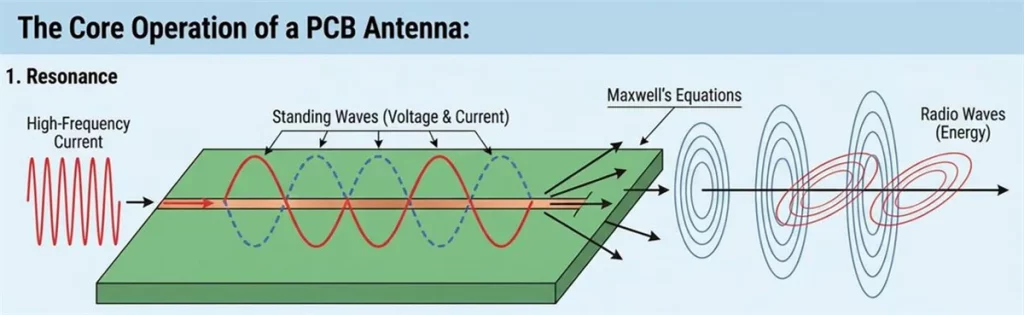
The core operation of a pcb antenna relies on resonance and Maxwell’s Equations. When high-frequency current travels along the trace, it establishes standing waves of voltage and current. Subsequently, this oscillation launches energy from the copper into free space as radio waves. To achieve this, the antenna length must strictly match a specific fraction of the wavelength (λ), usually 1/4 or 1/2.
Take a typical 2.4 ghz pcb antenna as an example. Its wavelength in free space is about 12.5 cm. However, the signal travels through the dielectric material of the PCB. This material has a dielectric constant (εr). It slows down the wave speed. Therefore, we must shorten the physical length of the antenna on pcb based on the “velocity factor.” This is why pcb antenna design requires extreme precision. Even a deviation of a fraction of a millimeter causes the frequency to drift away from the target.
Advantages of PCB Antennas
The pcb antenna has displaced external antennas in most high-volume consumer electronics.
- Cost-Free Manufacturing: Because manufacturers etch it during standard PCB fabrication, there is zero incremental BOM cost.
- Space Efficiency: It is essentially 2D, occupying no vertical height. This feature is critical for slim IoT sensors.
- Reliability: With no solder joints to fail or connectors to come loose, it offers superior mechanical durability.
- Customizability: Designers can shape the trace—meandering or curving it
Key Performance Parameters
Designing a pcb antenna is not merely an exercise in geometry; it is a battle against physics. To an engineer, the distinction between a high-performance antenna on pcb and a useless piece of copper lies in meeting specific electromagnetic metrics. Understanding these parameters is essential for validating your design.
Impedance (Input Impedance)
Definition: Input impedance (Zin) is the opposition to the flow of current at the antenna’s feed point. It consists of a real part (resistance, R) and an imaginary part (reactance, X), expressed as Zin= R + jX.
Standard: In the RF world, 50 Ohms (Ω) is the universal standard for transmission lines and transceivers.
The primary goal of matching is to make the antenna appear as a pure 50Ω resistor to the radio chip. If X ≠ 0 (inductive or capacitive), the antenna stores energy instead of radiating it. Conversely, if R ≠ 50, energy is reflected back to the source.
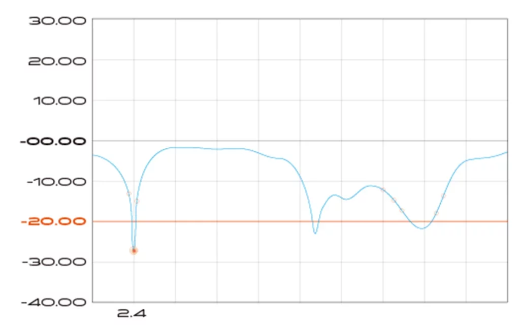
VSWR and Return Loss (S11)
These are the two most common metrics for measuring impedance matching. They quantify how much energy bounces back from the antenna because of a mismatch.
VSWR (Voltage Standing Wave Ratio):
VSWR measures the severity of the “traffic jam” on the transmission line.The ratio of peak voltage to minimum voltage in the standing wave pattern. A higher ratio means more severe reflection and wasted energy.
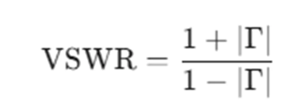
(Where Γ is the reflection coefficient)
Relationship between Reflection Coefficient and Impedance:

ZL:The load impedance (the antenna).
Z0:The characteristic impedance of the transmission line (cable or PCB trace), typically 50Ω.
Standard:
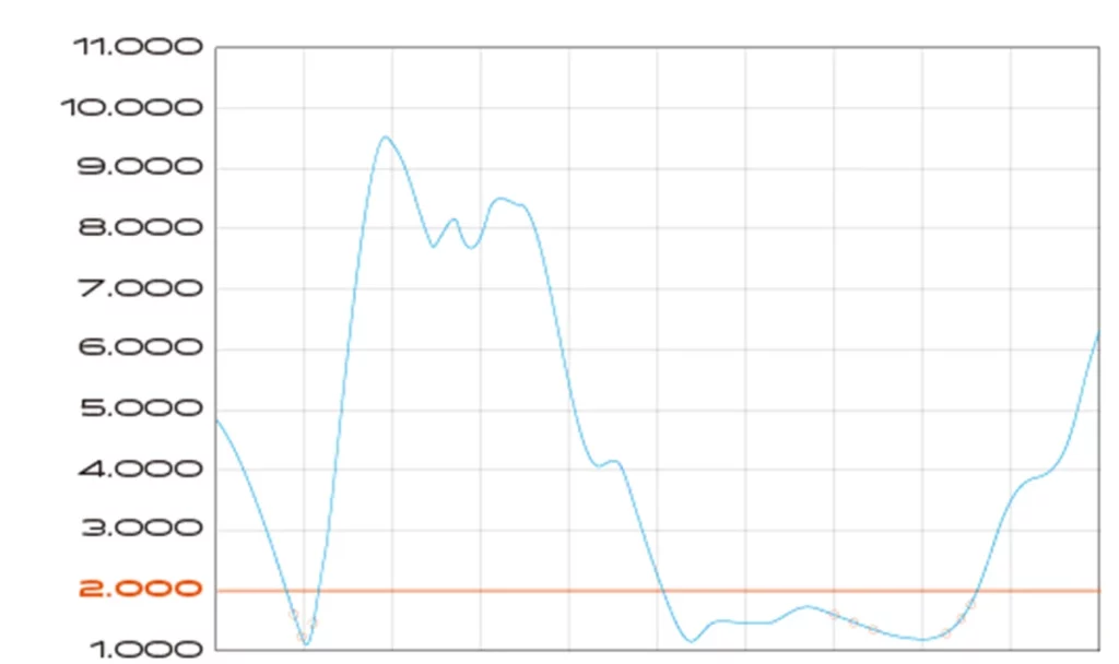
For a robust commercial product, the industry benchmark is a VSWR < 2.0 (equivalent to a Return Loss < -9.5 dB). At this level, the system delivers approximately 90% of the power to the antenna structure, ensuring efficient operation.
Return Loss (S11):
S11 represents the input power that reflects back. The lower the S11 value, the better the impedance match. In simple terms, it indicates how much energy bounces back because of a “roadblock” when you feed power into the antenna.
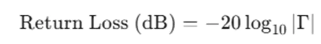
Numerical Characteristics: It is typically a negative number.
- 0 dB: Means 100% reflection. All energy is bounced back.(Terrible)
- -10 dB: Means 10% reflection, while 90% of the energy enters the antenna.(Qualified)
- -20 dB: Means 1% reflection, with 99% entering. (Perfect).
Curve Shape: On a VNA chart, S11 looks like an inverted valley (a V-shaped dip). The deeper the valley, the better the antenna performs at that specific frequency.
Radiation Efficiency
Definition: This is the ratio of the power actually radiated into space (Prad) versus the power delivered to the antenna input (Pin).
Equation:
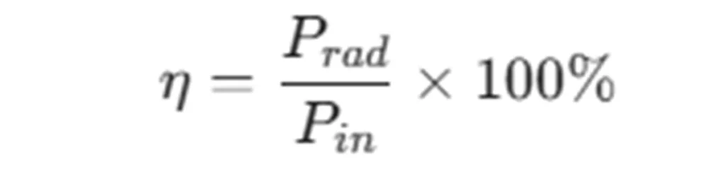
Significance:
This is the “health check” of your antenna. A pcb antenna might accept energy (good VSWR) but waste it as heat in the FR4 substrate. High efficiency means your battery power actually turns into a signal.
Performance Benchmarks:
- Excellent: > 70% (Typical for external dipoles).
- Good (PCB): 40% – 60%. For a compact pcb bluetooth antenna, 50% is a healthy target.
- Poor: < 20%. This results in significantly reduced range and wasted battery life.
Gain (dBi vs. dBd) and Directivity
Gain:
Functionally, gain is not just about “power increasing.” It describes how well the antenna converts input power into radio waves in a specific direction. To measure gain, we need a “reference point.” Depending on which reference is used, we get two different units:
- dBi: The gain relative to an ideal isotropic radiator. This is a theoretical, mathematical “point source” that does not exist in reality. It radiates energy equally in all directions (like a perfect sphere).
- dBd: The gain relative to a half-wave dipole. This is a real, standard wire antenna. A dipole naturally focuses energy (its radiation shape looks like a donut, not a sphere). A standard dipole already has a natural gain of 2.15 dBi over the isotropic sphere.
Conversion: 0 dBd= 2.15 dBi.
Directivity:
This describes the geometric shape of the radiation pattern. It represents how much the antenna concentrates energy in one direction, ignoring any material losses.
Equation: Gain=Directivity×Efficiency
Most pcb antenna designs are omnidirectional (Gain: 0 to 3 dBi). Do not blindly chase high gain. High gain means a narrower beam, which can cause signal loss in portable wearables when the user changes orientation.
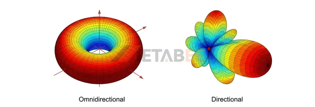
Radiation Pattern
Radiation Pattern defines how energy is distributed in space. Most PCB antennas (like in smart bulbs) are Omnidirectional, radiating a 360° “doughnut” of signal to connect from any angle. In contrast, Directional antennas focus energy like a flashlight beam, sacrificing width to gain range in a specific direction.
Bandwidth
Definition: Bandwidth refers to the effective frequency range where the antenna maintains a “VSWR < 2.0”.
A narrow bandwidth is dangerous. In the real world, factors such as variations in the FR4 substrate’s dielectric constant, inconsistent plastic casing thickness, or even glue differences during assembly can cause the antenna’s resonance frequency to drift. A wide bandwidth ensures the antenna stays tuned and operational despite these inevitable variations.
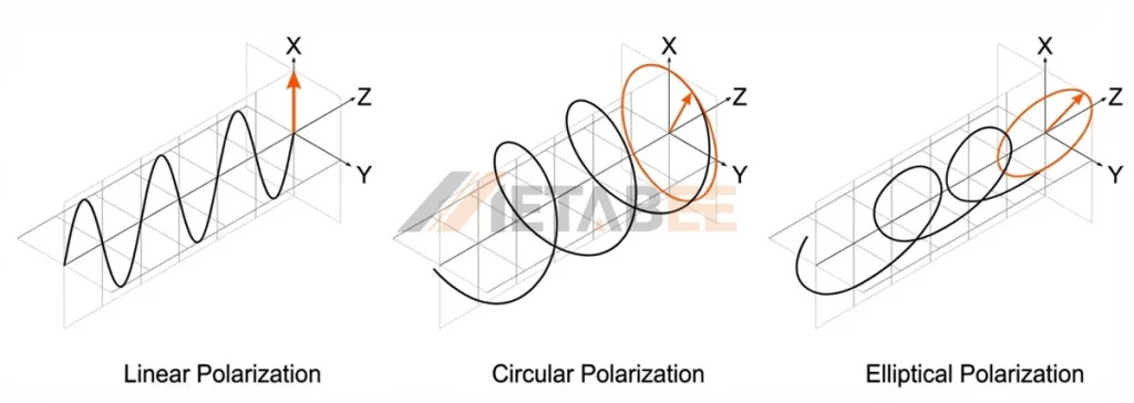
Polarization
Polarization describes the orientation of the radio wave’s electric field. It can be linear or circular. Most PCB antennas are linearly polarized (vertical or horizontal).
Imagine trying to throw a frisbee through a fence. If you throw it flat (horizontal) and the fence slats are vertical, the frisbee gets blocked. In wireless engineering, antennas work the same way. The transmitting and receiving antennas must share the same alignment (polarization). If they are crossed—one vertical and one horizontal—the signal creates a “cross-polarization loss” and communication fails.
- Linear polarization: commonly used in ground-based mobile antennas.
- Circular polarization: used in GPS antennas to counter multipath and rotation effects.
Types of PCB Antennas: A Market Perspective
In the commercial market, we categorize pcb antennas based on their integration level and design complexity.
Embedded Trace Antennas
This is the most common category for high-volume products. Designers draw the antenna simply as a copper trace directly on your circuit board layout.
- Inverted-F Antenna (IFA): The undisputed market leader. It looks like the letter “F”. Due to its compact size and easy tuning, it is widely used for pcb bluetooth antennas, balancing size and efficiency perfectly.
- The Meandered Trace (MIFA): When space is extremely tight, engineers fold the copper line back and forth like a snake. This is common in 433mhz pcb antenna designs where the wavelength is long. It saves space but sacrifices some bandwidth.
- Features: These are “free” to manufacture but require expert pcb antenna design skills to simulate and tune.

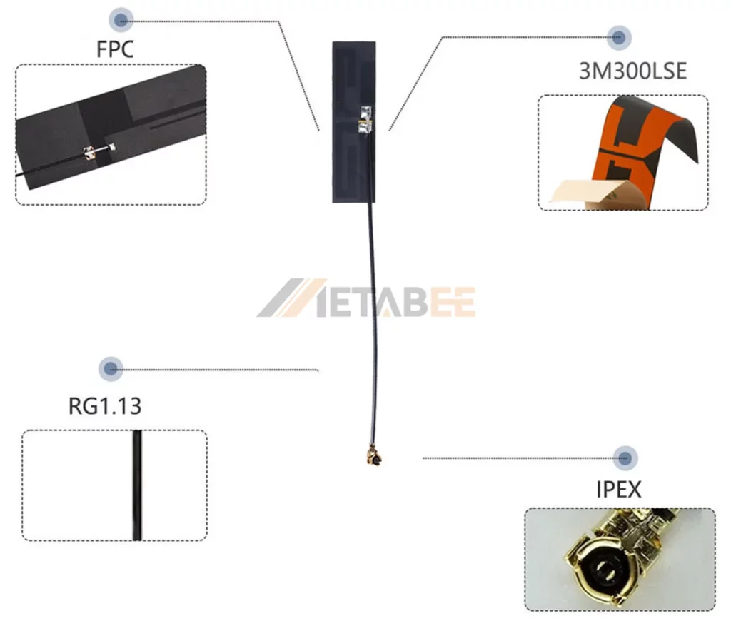
Off-the-Shelf FPC Antennas
If you search for “PCB Antenna” on a distributor website, this is what you find. These are pre-made flexible pcb antennas sold by companies like Molex or TE Connectivity.
- Shape: They look like small stickers with a cable and a U.FL/IPEX connector.
- Usage: You simply peel the adhesive backing and stick it to your device’s plastic housing. Then, plug the cable into your radio chip.
- Features: They are more expensive per unit than a trace. However, they eliminate the risk of RF layout errors. They are ideal for projects that need to get to market quickly without RF experts.
FPC antenna structure diagram
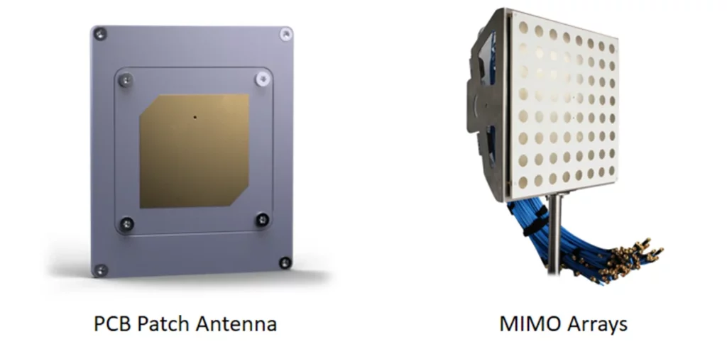
Patch & Array Antennas
This category serves the high-speed and satellite markets.
- PCB Patch Antenna: A rectangular “patch” of copper used primarily for GPS/GNSS or high-frequency radar. It is directional, looking up at the sky.
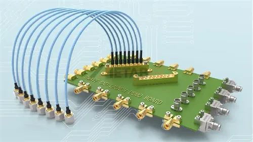
- MIMO Arrays: Essential for modern communication. A 5g pcb antenna is rarely a single wire. It is a cluster of multiple radiators working together. These use complex multi-layer structures to handle massive data throughput.
- Features: These represent the cutting edge. They often require specialized, low-loss PCB materials (like Rogers) instead of standard FR4 to function correctly.
Which Antenna is Best for Your Device? A Comprehensive Comparison
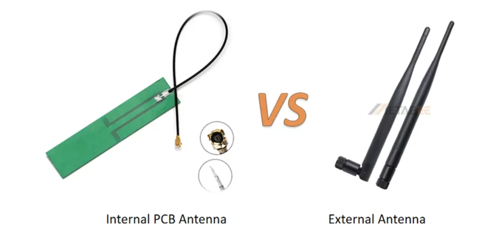
Selecting between an internal pcb antenna and an external antenna is a strategic decision that affects range, aesthetics, and regulatory certification (FCC/CE).
PCB Antenna vs. External Antenna
The debate of pcb antenna vs external antenna is fundamentally a choice between aesthetics and range.
- External Antenna (Rubber Duck): An external wifi antenna or external radio antenna sits outside the device’s metal noise and plastic housing. This provides a “cleaner” signal path and higher gain. For example, for industrial gateways requiring a 5km range, you must use a 5g external antenna.
- Internal PCB Antenna: While it may have lower peak gain due to enclosure interference, the pcb antenna is protected from the elements and maintains the device’s sleek industrial design.
FPC vs. PCB (Rigid)
In the fpc vs pcb comparison, FPC offers a distinct advantage in RF isolation. An antenna fpc can be adhered to the plastic housing, positioning it far away from the noisy CPU and power lines on the main board. Consequently, it often performs better than a rigid antenna on pcb that is stuck in a crowded layout.
PCB vs. Chip Antenna
While chip antennas save incredible amounts of space, they have downsides: higher cost and narrower bandwidth. Therefore, only choose a chip if your device is too small for a printed trace. For most designs, a standard pcb antenna is the superior choice because it provides better efficiency for free.
| Feature | PCB Trace Antenna | Chip Antenna | FPC Antenna | External Antenna |
| Cost | Lowest (Zero BOM) | Medium ($0.10 – $1.00) | High ($0.50 – $2.00) | Highest ($2.00+) |
| Size | Large (Requires length) | Tiny (Ceramic shrinks size) | Flexible (Fits anywhere) | Bulky (External rod) |
| Performance | High (Good bandwidth) | Medium (Narrow bandwidth) | High (Good isolation) | Best (Max Range) |
| Design Effort | High (Simulation needed) | Low (Drop-in component) | Low (Plug & Play) | Low (Screw-on) |
| Best For | High-volume IoT, Smart Plugs | Earbuds, Smartwatches | Curved Wearables, VR | Industrial Gateways |
Common Applications
Wearables and Consumer Electronics
In the wearable market, every millimeter counts. Designers use the flexible pcb antenna to wrap around the battery. The bluetooth pcb antenna is the heart of every TWS earbud, requiring clever “meandered” designs to fit into a tiny ear tip.
Smart Home and Building Automation
The 2.4 ghz pcb antenna is ubiquitous in smart bulbs, plugs, and sensors. However, in luxury homes with thick walls, a designer might supplement the device with an external radio antenna or a high-gain external antenna for wifi to ensure the signal reaches the basement.
Automotive and Telematics
Modern cars are essentially rolling mobile phones. They contain 4g pcb antenna arrays for GPS and LTE, and increasingly, 5g pcb antenna modules for V2X (Vehicle-to-Everything) communication. While the radio might use an external fm antenna, the high-speed data is handled internally.
How to Design PCB Antenna?
Designing a high-performance antenna is where science meets art. If you want to know how to design pcb antenna, you must follow a rigorous RF workflow.
Need Help Tuning Your Design?
Antenna design is complex, and simulation software is expensive. If you need a custom layout, contact our engineering team. We can help simulate and fine-tune your design to ensure peak performance before you go to mass production.
Step 1: Specifying its type
Define your Operating Frequency, Bandwidth, and Space Constraints first.
- Space-Constrained: The Inverted-F Antenna (IFA) or Meandered IFA (MIFA) are preferred. They utilize PCB edge space effectively.
- Omnidirectional: The Monopole Antenna offers high efficiency but requires a larger clearance area.
Step 2: Calculating the size
You cannot simply use the speed of light in a vacuum to calculate the trace length. Because the antenna is a copper trace on a substrate (Microstrip), the radio wave travels through a mix of Air(εr≈1.0) and FR4(εr≈4.4).
You must calculate the Effective Dielectric Constant (εeff), which represents this “mixed” environment.
The Physics Formulas:
1. First, calculate the wavelength (λ0) of your target frequency in free space (air).

c: Speed of light (3×10⁸m/s)
f: Target frequency (in Hz)
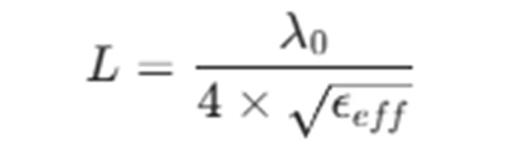
2. Required Antenna Length (L):
For a λ/4 printed monopole antenna, the length is:
Step 3: Layout
- Placement: Place the antenna at the corner or edge of the PCB to minimize obstruction by the ground plane.
- Keep-Out Area: The area directly above and below the antenna radiator (on all layers) must be free of copper and traces to prevent parasitic capacitance and frequency detuning.
- Ground Plane: Ensure a solid, continuous ground plane. Add dense Via Stitching along the ground edges to create a stable reference.
Step 4: Simulation Testing
Simulation often deviates from reality; a Pi-network (π-network) must be reserved for matching.
- In-Housing Tuning: Plastic enclosures act as a dielectric, shifting the resonant frequency lower (Detuning).
- Trimming Method: Use a Vector Network Analyzer (VNA) to monitor Return Loss (S11). If the frequency is too low, physically cut/trim the antenna tip to shift the frequency up until S11 < -10dB.
Why Choose Metabee for Your Antenna Solutions?
At Metabee, we believe reliable connectivity starts with premium materials. Our FPC and PCB antennas are built with precision materials and rigorous testing standards to ensure your device stays connected.
Key Product Features:
- high quality materials
- imported raw materials high strength/ uv resistant
- light weight antenna
- small product size
- light weight
- non-deformable
- high dielectric constant
- strict product testing
- improted instruments products are tested by network analyzer

Conclusion
The pcb antenna represents the perfect convergence of physics and economy, offering a low-cost solution for high-performance wireless connectivity. From selecting the right topology (IFA vs. MIFA) to mastering the nuances of impedance matching and net clearance, every decision impacts your product’s range and reliability. A well-executed pcb antenna design transforms a simple circuit board into a powerful communication device.
Need a Tailored RF Solution?
Standard designs don’t fit every housing. Metabee specializes in custom pcb antenna services to match your unique mechanical and performance requirements. Contact us today, and let’s engineer the perfect signal for your product.
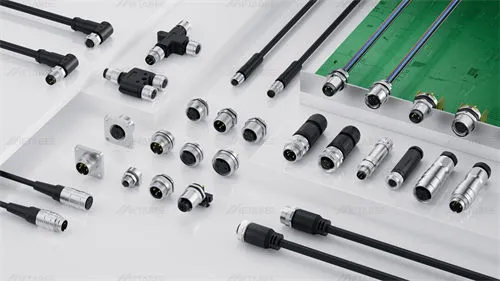
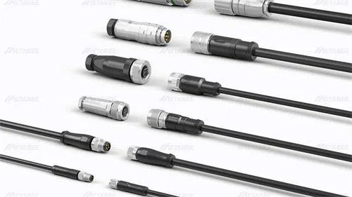
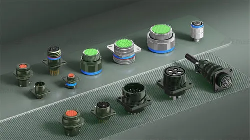
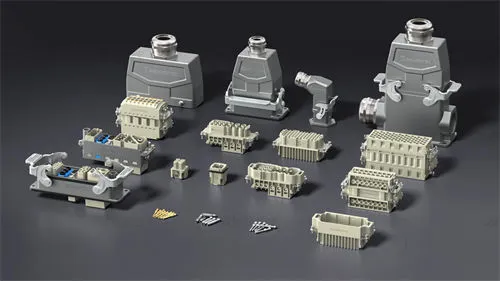
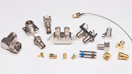
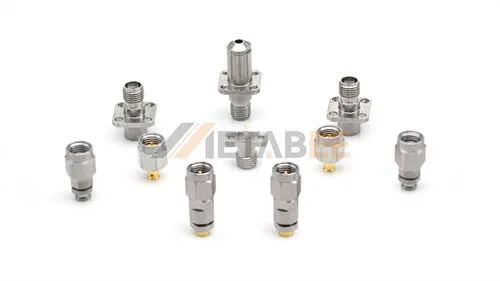
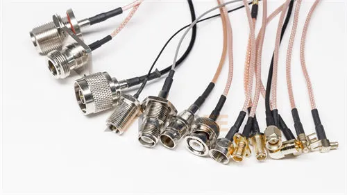
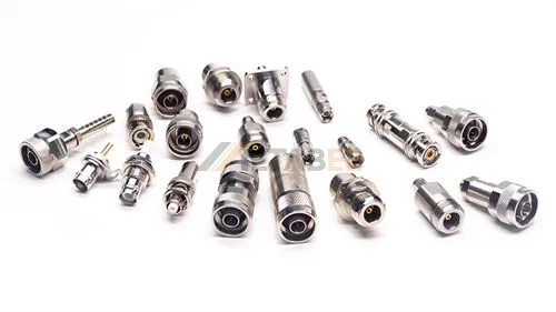
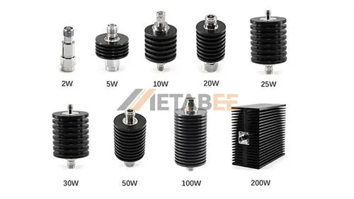
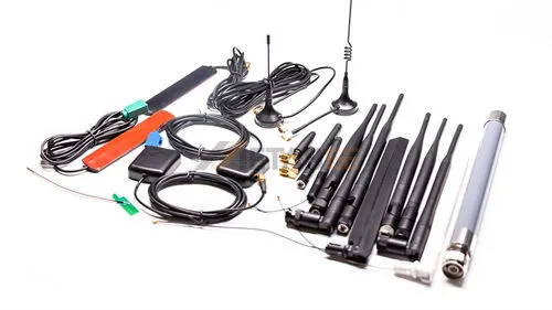
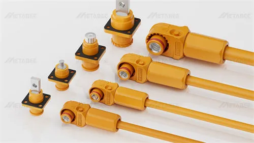
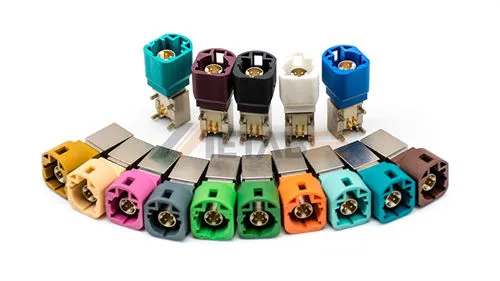
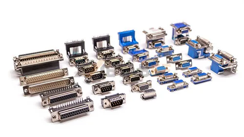
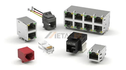
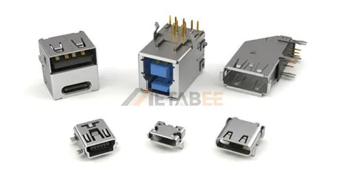
Related Product
FAQs
Q1: What about Chip Antennas?
A: While often discussed alongside PCB antennas, a Chip Antenna is actually a separate ceramic component soldered onto the board. It is not etched from the PCB copper itself. Engineers use it when there isn’t enough space to draw a full PCB trace antenna.
Q2: What is the difference between a PCB antenna and an external rubber duck antenna?
A: A PCB antenna is integrated directly into the device (etched on the board or FPC), making it compact and low-cost. An external antenna is a separate rod that screws onto the outside, offering better range but adding bulk and cost.
Q3: Embedded PCB antenna vs. external antenna, which signal is better?
A: In terms of pure physics, the external antenna generally offers a better signal. Its larger size allows for higher gain, and its physical separation from the noisy circuit board (CPU/Memory) reduces interference. However, for most consumer IoT devices, a PCB antenna offers “good enough” performance with a much sleeker design.
Q4: Why is my PCB antenna range so short?
A: The most common culprit is a poor ground plane or incorrect impedance matching. If the antenna isn’t tuned to 50 Ohms, energy reflects back instead of radiating. Also, placing the antenna too close to metal components (like batteries) will severely detune it.